In-operando Angle Resolved Photoemission Spectroscopy (ARPES) With Spatially High Resolution
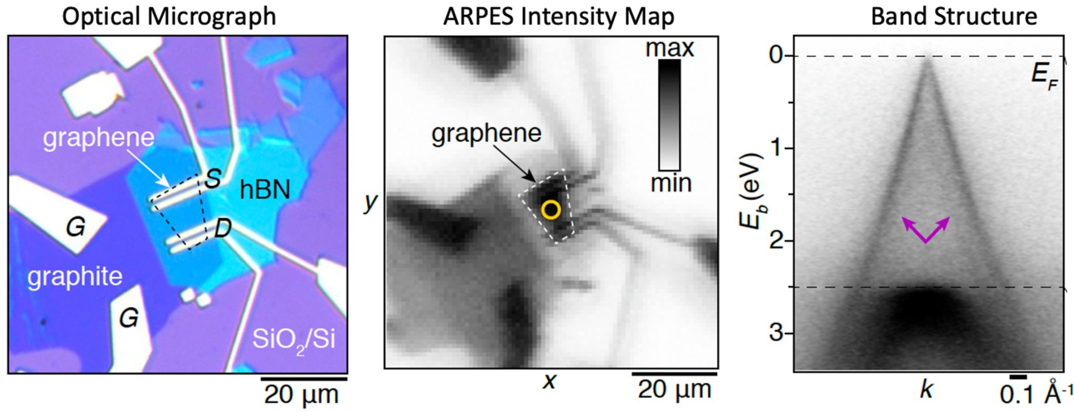
Our group utilizes ARPES with focused spot size to directly probe the energy-momentum information of mesoscopic sized high-quality single-layer exfoliated 2D materials and their heterostructures and devices. We have an approved program (AP) to probe the electronic band structure of 2D based devices using the state-of-the-art in-operando nanoARPES (with spatial resolution reaching 120 nm) at MASTERO beam line at Advanced Light Source (ALS), Berkeley. With the advent of nano-ARPES, the exploration of exotic physical phenomenon in the vast library of emerging 2D materials, van der Waals heterostructures, and devices is just the beginning!!!
Synthesis of Topological Materials
Molecular Beam Epitaxy
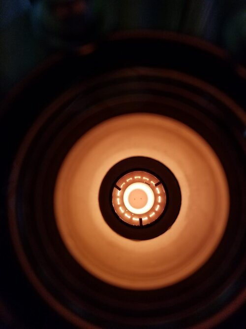
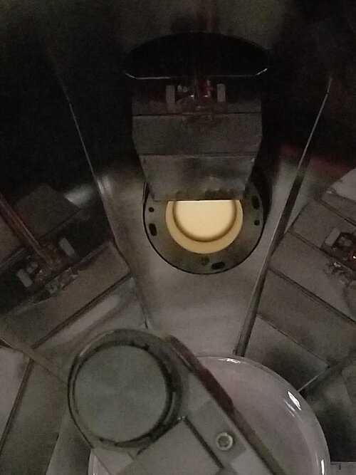
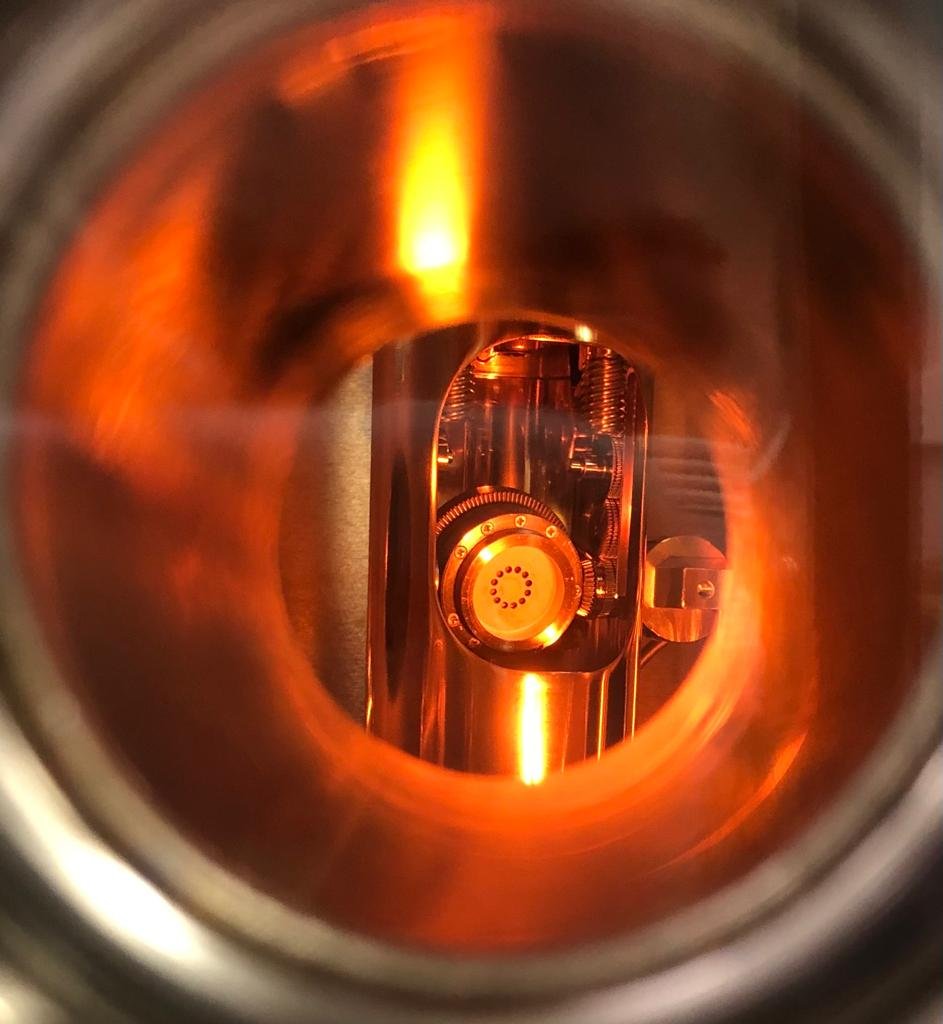
There is an increasing demand for synthesis of high quality novel quantum materials with exotic properties. Molecular beam epitaxy (MBE) is an excellent technique to grow crystalline thin films by deposition of atoms or molecules layer-by-layer onto a substrate. The advantages of MBE over other growth methods include better control of doping, uniformity of epitaxial film thickness, and sharp crystalline interfaces in heterostructures. Our focus is to grow variety of materials including: 2D Si/Ge/Sn, graphene analogues, topological Dirac 3D semimetals, complex oxide thin films & hetero-interfaces, and magnetic thin films (in Collaboration with Singh group). Some of these materials are predicted to exhibit exotic topological phases, such as near-room-temperature quantum anomalous Hall effect and topological superconductivity. In addition, we intend to tune the band gap and SO coupling in these materials by surface functionalization and alloying.
van der Waals hetero-structures and interfaces
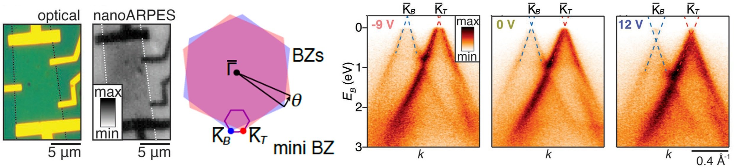
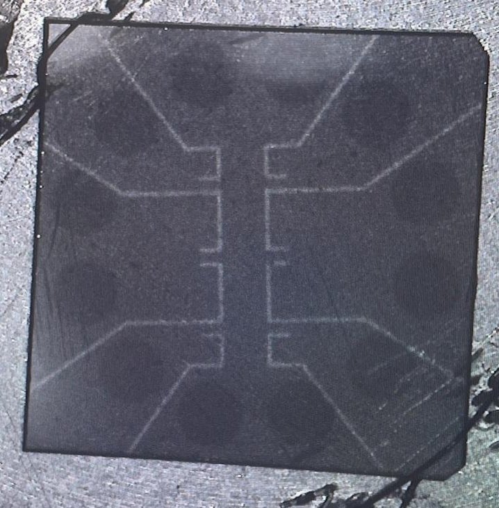
The experimental technique to mechanically assemble extremely clean interfaces of arbitrary atomically thin sheets of van der Waals (vdW) materials provides unprecedented flexibility to control the physical properties, modify spin-orbit coupling and band structures, and induce magnetic and topological correlations by proximity effects at the atomic limit. We use van der Waals based transfer technique, in a controlled environment, to assemble 2D/2D, 2D/3D, 2D/1D cross-dimensional hetero-structures to study the electronic, spin and optical properties of these systems. We are also developing a transfer tool to assemble cross-dimensional material hetero-structures in ultra high vacuum to exploit the true potential of intrinsic phenomena that emerge at atomically clean interfaces.
The material synthesis and interface engineering provides us the ability to investigate novel physics phenomena in vast class of quantum materials using ARPES, in-situ magneto-transport, magnetization dynamics and optical techniques.
In-operando Tuning of Material’s Properties
Being atomically thin, the effects of surface adsorption, electrostatic gating, Coulomb interactions, strain, and proximity-induced phenomenon are more pronounced in 2D materials than their 3D counterparts. However, the ‘all surface’ nature of 2D materials also makes these materials extremely sensitive to their surrounding environment, which can be detrimental to their ground state intrinsic properties. This presents a fundamental challenge to the utility of 2D materials for future technological applications. Thus, it is imperative to fully understand the role of extrinsic perturbations on the intrinsic properties of 2D materials. This knowledge will produce two critical breakthroughs in this field: firstly, it elucidates a fundamental understanding of how to systematically remove extrinsic effects in order to fully exploit the intrinsic properties of 2D materials, and secondly, it allows us to tune the properties of 2D materials through extrinsic effects by simply modifying their environment. Our research in this direction is driven by the following open questions in the field of 2D materials:
1) What effects do external perturbations (mechanical stress, chemical environment, electrostatic interactions, etc.) have on the electronic, optical, valley, and spin-related properties of 2D materials?
2) How can we utilize surface modification and substrate engineering to alter the physical properties in 2D materials?
We utilize in-situ magneto-transport and optical measurements to study the quantum phenomenon in mesoscopic sized 2D material devices while doping (or changing the surrounding environment) it with adatoms.